
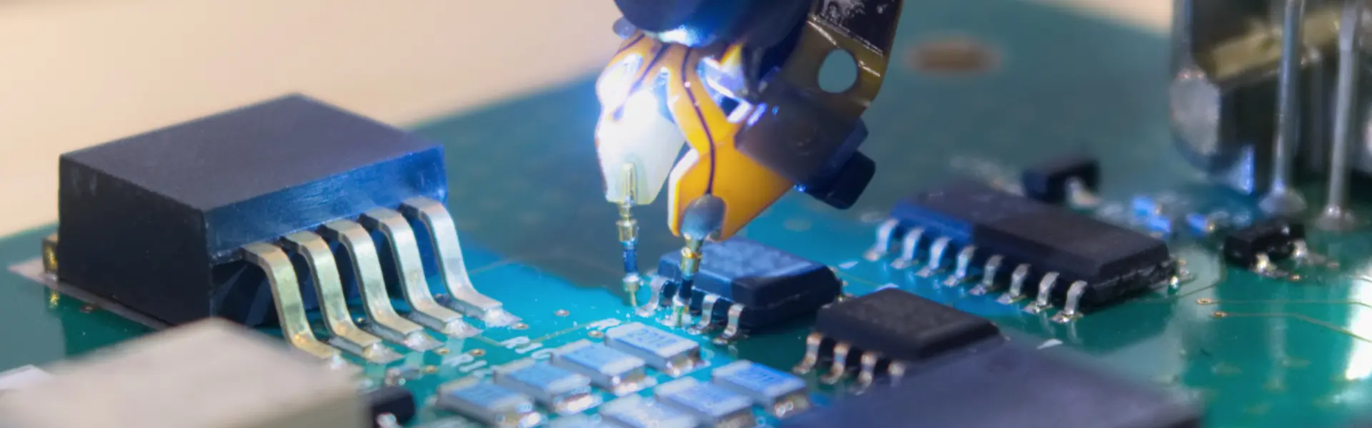
India’s semiconductor programme has spent four years being described in the future tense. Approvals, foundation stones, memoranda of understanding and artist impressions of cleanrooms. In 2026 that language has finally begun to change. Three plants are packaging chips commercially, a fresh wave of projects has been cleared across six states, and the Union Cabinet has approved a second and much larger phase of the mission.
For investors, the question is no longer whether India will build a chip ecosystem. It is which parts of that ecosystem are actually reaching commercial production, and which listed companies capture the spending along the way.
Table of Contents
What Has Changed?
On 15 July 2026 the Union Cabinet approved the India Semiconductor Mission 2.0, also called Semicon 2.0, with an outlay of Rs. 1.27 lakh crore. It was cleared alongside a Rs. 62,500 crore Mobile Phone Manufacturing Scheme, taking the combined electronics package to roughly Rs. 1.9 lakh crore.
The design of the incentive has changed more than the headline number has.
- Silicon fabs now receive support of up to 40 per cent of project cost, against a uniform 50 per cent under the first phase
- Compound semiconductor, discrete and display fabs receive up to 35 per cent
- Manufacturers of semiconductor equipment, chemicals, gases and materials receive a flat 30 per cent
- Chip design is supported through a mix of grants and equity investment rather than capital subsidy alone
The government expects the mission to eventually draw around Rs. 4 lakh crore of investment, Rs. 2 lakh crore of production and Rs. 1 lakh crore of exports. The Union Budget for 2026-27 released an initial Rs. 1,000 crore, with the balance staggered across the programme.
Why the Government Has Widened the Net
1. Fabs Alone Do Not Make an Industry
A chip plant is only as reliable as the ultra-pure gases, photoresists, slurries, substrates and precision tools feeding it. India imports almost all of this.
2. Cost and Lead Time
Importing every consumable adds freight, duty and weeks of lead time to a business where unplanned downtime is ruinously expensive.
3. Value Capture Rather Than Assembly
The smartphone incentive programme taught a hard lesson. India scaled volumes handsomely, but domestic value addition stalled well below target. Semicon 2.0 is an attempt not to repeat that with silicon.
4. Strategic Autonomy
Compute, memory, power, radio frequency and sensor chips have been identified as building blocks for strategic requirements, including defence and telecom.
Grow your wealth with Bonanza
From Paper Plans to Packaged Chips
The back end of the value chain is where the change is already visible.
- Micron’s assembly and test facility at Sanand began operations in February 2026
- Kaynes Semicon’s outsourced assembly and test unit at Sanand followed in March 2026
- CG Semi, a subsidiary of CG Power, began commercial production at Sanand in July 2026 with roughly 20 crore units of annual capacity
Sanand has effectively become India’s first chip packaging cluster. Gujarat alone now hosts six approved projects representing about US$ 14.7 billion of investment, and the wider mission counts 12 approved units across six states with a cumulative pipeline above Rs. 1.60 lakh crore.
The sequencing is sensible. Packaging plants cost a fraction of a wafer fab, ramp in months rather than years, and build the skilled workforce a fab will later need.
The Fab Is the Harder Half
Front-end wafer fabrication remains the unfinished piece.
The Tata Electronics and PSMC project at Dholera, a Rs. 91,000 crore facility designed for 50,000 wafers a month, was originally guided to produce its first chip in December 2026. Commercial operations are now expected around mid-2028. The plant is also expected to begin with mature 90nm and 55nm nodes before introducing 28nm.
This deserves to be read carefully rather than dramatically. Phased node introduction is standard practice, and 28nm remains commercially vital. But it does mean the revenue, and the domestic supply chain pull, from India’s first fab arrive later than the market had assumed.
Immediate Market Reaction
Following the Cabinet approval, semiconductor and electronics manufacturing stocks rallied. Cyient DLM, Dixon Technologies, PG Electroplast, Kaynes Technology and Syrma SGS all gained on the announcement day.
The move reflected sentiment rather than earnings. Very little of this outlay converts into revenue for listed companies inside the current financial year.
Where the Listed Exposure Actually Sits
1. Direct Manufacturing
- CG Power and Industrial Solutions, through its majority-held CG Semi venture with Renesas of Japan and Stars Microelectronics of Thailand
- Kaynes Technology, through Kaynes Semicon at Sanand
- HCL Technologies, through its packaging joint venture with Foxconn at Jewar in Uttar Pradesh
- Archean Chemical Industries, whose step-down subsidiary is building India’s first approved silicon carbide fab at Bhubaneswar for about Rs. 2,067 crore
2. Design and Engineering Services
Chip design is where India already has genuine depth. Listed exposure runs through Tata Elxsi, Larsen and Toubro via its semiconductor arm, MosChip Technologies, Cyient DLM, Syrma SGS Technology and SPEL Semiconductor.
3. Chemicals, Gases and Materials
This is the segment ISM 2.0 has deliberately opened up, and the flat 30 per cent incentive is aimed squarely at it. Companies with relevant chemistry or supply relationships include Linde India in industrial and specialty gases, and fluorochemical producers such as Navin Fluorine, Gujarat Fluorochemicals and SRF.
One caveat matters enormously here. Electronic-grade purity is a different specification from industrial grade, and qualification cycles run for years. Presence in the chemistry is not the same as presence in the fab.
4. Construction and Infrastructure
Every plant needs land development, structures, cleanrooms, high-purity piping, power and water. Tata Projects has been the engineering, procurement and construction contractor on Tata group semiconductor sites, with listed suppliers such as Interarch Building Products winning pre-engineered building orders. Cleanroom engineering itself has gone largely to overseas specialists.
Why This Is Not a Straight Line
- India still imports more than 90 per cent of its semiconductor equipment and most specialty materials
- Central support per project is lower under phase two, with states expected to carry a larger fiscal share
- Yield, not installed capacity, decides fab economics, and yield takes years to mature
- Order flows for ancillary suppliers are lumpy and tied to construction schedules that slip
What to Monitor
- Detailed scheme guidelines and notified eligibility for the equipment and materials incentive
- Capacity utilisation and customer wins at the three operating packaging units
- Construction milestones at Dholera and Jagiroad
- Order announcements from listed construction, gas and chemical suppliers
Investment Outlook
a. Near Term. Sentiment Driven
Policy news moves these stocks well before it moves their profit and loss statements.
b. Medium Term. Execution Specific
Differentiate between companies with commissioned assets and companies with announcements. The first group has revenue visibility. The second has optionality.
c. Long Term. Structurally Positive
India’s semiconductor demand is expected to roughly double towards US$ 100 billion by the end of this decade. An ecosystem serving even a modest share of that is a large business.
Conclusion
ISM 2.0 marks the point at which India’s chip policy stopped being about landing a marquee fab and started being about building the plumbing around it. Packaging is genuinely commercial today. Design has always been a strength. Materials, gases, equipment and construction are the new frontier, and that is precisely where the incentive money has moved.
The honest counterpoint is that fabrication, the piece that anchors everything else, is still roughly two years away, and the first plant will begin on mature nodes. Investors buying this theme are buying a decade, not a quarter.
Bottom Line. The transition from paper plans to commercial production is real, but it is happening back to front. Packaging first, materials next, wafers last. Companies with operating assets and qualified customers deserve to be valued very differently from those holding press releases, and that distinction will matter far more to returns than the size of the outlay.
You can also join our community at LinkedIn, Instagram, and Twitter to stay updated.
Latest Posts
-
 11 Aug 2026
Why Every Vehicle Owner Should Know About the Supreme Court’s New Insurance Proposal?
-
 10 Aug 2026
UPI Charges Are Coming? What The New Parliament Bill Actually Means For You
-
 06 Aug 2026
Stock Market Timing Has Changed From 03 August: All You Need to Know
-
 04 Aug 2026
Emergency Fund: The 3-6-9 Rule Every Investor Should Know!
Related Posts
-
 30 Jul 2026
India Bonds on Edge: What the Market Is Really Watching For?
-
 28 Jul 2026
NITI Aayog’s Investment Friendliness Index 2026: All You Need to Know
-
 23 Jul 2026
Pharma Tariffs: A New Era of Protectionism – Impact on Indian Pharmaceutical Companies and the Road Ahead
-
 22 Jul 2026
RBI’s Forex Swap Scheme Has Raised $20.72 Billion: All You Need to Know





 Invest Now